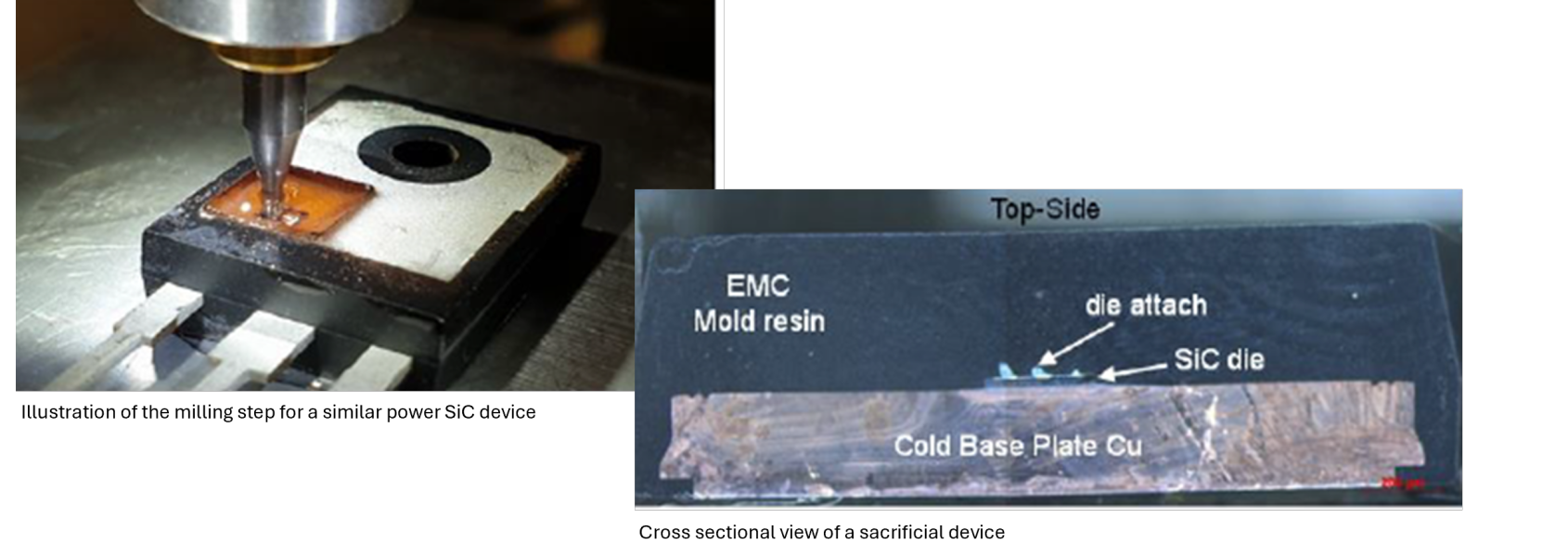
At ISTFA, Rosine GERMANICUS presented a paper about "SiC MOSFET micro-explosion due to a Single Event Burnout: analysis at the device and die levels". We at JPK Group are proud that we could support this paper with sample preparations conducted with a micro milling tool from our principle ULTRA TEC.
Please contact us for the complete paper or interest in Failure Analysis, Sample Preparation or FA Workshop on January 31, 2024 in Munich.
Contact: sales_de@jpkummer.eu
For device qualification in harsh environments (space, avionic and nuclear), radiation testing identifies the sensitivity of the devices and technologies and allows to predict their degradation in these environments. In this paper, the analysis of the electrical characteristics and of the failure of a commercial SiC MOSFET after a Single Event Burnout (SEB) induced by proton irradiation are presented. The goal is to highlight the SEB degradation mechanism at the device and die levels. For failed devices, the current as a function of the drain-source bias (VDS) in off-state (VGS=0V) confirms the gate rupture. For the die analysis, Scanning Electron Microscopy (SEM) investigations with energy-dispersive X-ray spectroscopy (EDX) analysis reveals the trace of the micro explosion related to the catastrophic SEB inside the SiC die. With a fire examination, similar to a blast, the SEM analysis discloses damages due to the large local increase of the temperature during the SEB thermal runaway, leading to the thermal decomposition of a part of the SiC MOSFET and the combustion with gaseous emissions in the device structure.


 We are deligthed at JPK Group to announce our new partnership with SOLARIUS. SOLARIUS is a leading provider of precision systems for non-contact surface inspection, measurement, analysis, and visualization. The product portfolio combines high-resolution sensors with automated data acquisition systems and powerful analysis tools. Offerings range from desktop systems for off-line inspection, to semi-automated systems for fast, precise measurements, to customized multi-station platforms for high-volume in-line inspection.Based on experience in various fields, we use this technology for Optical Probe Card Inspection. If you are either looking for cyclic routine inspection, new card income inspection or post maintenance check-up, SOLARIUS will be able to support your application request. Our target: A fast probe card inspection enabling a clear and resilient decision if a probe card is OK for testing or NOT.